
CVD Diamond Manufacturer
CVD Diamond Wafer Manufacturer for Semiconductor, Photonics & Advanced Thermal Applications
High-purity synthetic CVD diamond with thermal conductivity up to 2200 W/m·K for next-generation electronic, optical, and quantum systems.
Maitri’s Q2 Diamonds manufactures CVD diamond wafers, substrates, and engineered diamond materials for semiconductor, RF, photonics, and high-power electronics applications.
Request Technical ConsultationDatasheets, samples, and technical discussions available for OEMs, research labs, and device engineers.
- ✔ CVD diamond wafers and substrates
- ✔ Thermal conductivity up to 2200 W/m·K
- ✔ Semiconductor, photonics & quantum applications
- ✔ Custom geometries, thickness & surface finishing
- ✔ Scalable manufacturing with cost advantage
What is CVD Diamond?
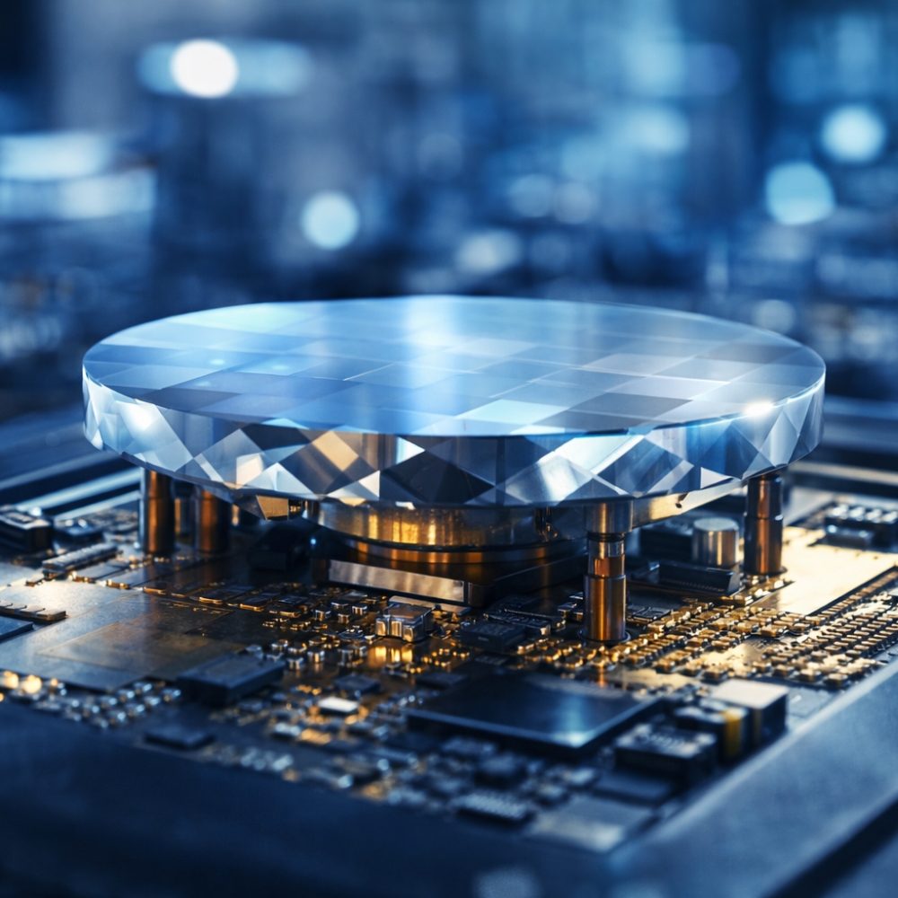
Chemical Vapour Deposition (CVD) diamond is a synthetic diamond material engineered through controlled deposition of carbon atoms onto a substrate under high-temperature plasma conditions, with CVD standing for Chemical Vapor Deposition. Compared with natural diamonds, CVD diamonds are produced using chemical vapor deposition, typically show fewer flaws, and offer more consistent quality.
CVD diamond is widely used in semiconductor substrates, photonics components, RF devices, and advanced thermal management systems where performance limits of conventional materials such as copper, aluminium, and silicon are exceeded.
As a high thermal conductivity material, CVD diamond enables efficient heat spreading, reduced thermal resistance, and improved system reliability in high-power and high-frequency environments.
Why Use CVD Diamond Materials?
Ultra-High Thermal Conductivity
Up to 2200 W/(m·K), with exceptional thermal conductivity that is significantly higher than common metals used for thermal control. This supports efficient heat dissipation in high-power semiconductors while CVD diamond can efficiently transport heat and maintain electrical insulation.
Semiconductor Compatibility
Low CTE improves integration with GaN, SiC, and advanced devices, making the material suitable for semiconductor technology not only as a substrate but also as a heat-spreading layer underneath semiconductors. Its wide bandgap of about 5.5 eV is an added benefit in demanding electronic applications.
Electrical Insulation
Ideal for RF, microwave, and high-frequency electronics, where this combination supports heat transport while maintaining electrical insulation, and its electrical properties matter for device performance.
Optical Performance
Used in photonics, laser systems, and optical applications, with optical transparency from UV to IR that makes them suitable for advanced optical components. In high-power systems, these wafers can serve as both heat spreaders and optical windows.
Extreme Environment Stability
Operates reliably in aerospace, defence, and high-temperature systems, with strong temperature stability, chemical inertness, and resistance to chemical degradation in harsh environments. Its high hardness and wear resistance, along with erosion resistance, support long service life in abrasive or corrosive conditions.
Precision Engineering
Custom thickness, polishing, and metallisation available, with precision engineering in the process also allowing control of crystal orientation for application-specific performance; polishing, metallisation, and surface coating can be customised for specific applications.
Applications of CVD Diamond
Semiconductor Substrates
Diamond substrates for GaN, SiC and high-power devices, where they are used beneath GaN and SiC components to improve thermal management in high-power electronics and support electronic devices.
RF & Microwave Devices
Thermal management for amplifiers and radar systems, where RF and microwave assemblies use diamond as heat spreaders to stabilise amplifiers and radar electronics under high power density.
Photonics & Optics
Optical-grade diamond for optical applications such as laser windows in laser systems, where thermal control and durability matter. It is also used in high-power lasers as optical components that manage heat while maintaining precision.
Quantum Technologies
Diamond materials for NV centres, quantum research, and quantum computing. CVD diamonds can also be engineered with controlled impurities to create NV centres used in quantum sensors and related devices.
High-Power Electronics
Heat dissipation in compact, high-density systems, making the CVD diamond wafer suitable for high-power electronics, optics, and quantum technologies.
Aerospace & Defence
Reliable materials for extreme operational environments.
CVD Diamond Products & Capabilities
CVD Diamond Wafers
High-purity wafers for semiconductor and photonics integration, available in single crystal diamond or polycrystalline formats depending on device requirements, with scalable production to support wafer supply.
Diamond Substrates
Engineered substrates for thermal and electronic applications, used beneath semiconductors in high-power packaging to improve efficient heat dissipation; CVD diamond wafers provide superior heat dissipation for high-power semiconductors.
Optical Grade Diamond
Polished diamond for optical and laser systems.
Metallised Diamond
Ready-to-integrate substrates for packaging and assembly.
- Custom sizes and geometries
- Single crystal and polycrystalline CVD diamond
- Surface polishing and finishing
- Scalable manufacturing capability
Work with Q2 Diamonds
We support semiconductor companies, research institutions, and advanced engineering teams with high-performance CVD diamond materials tailored to demanding applications.
From prototyping to volume production, Q2 Diamonds delivers scalable, cost-efficient synthetic diamond manufacturing with engineering support across global markets, meeting rising demand as this technology advances for sustainable energy systems, environmental processes, and future applications.
Production remains 100–250 times more energy-intensive than silicon, but CVD diamonds can still be considered green when made with renewable energy — the process can use methane and hydrogen without CO2 emissions, while remaining more cost-effective than HPHT methods.
Discuss Your Application

71–75 Shelton Street, Covent Garden, London, United Kingdom, WC2H 9JQ
Company Registration No: 16821217