
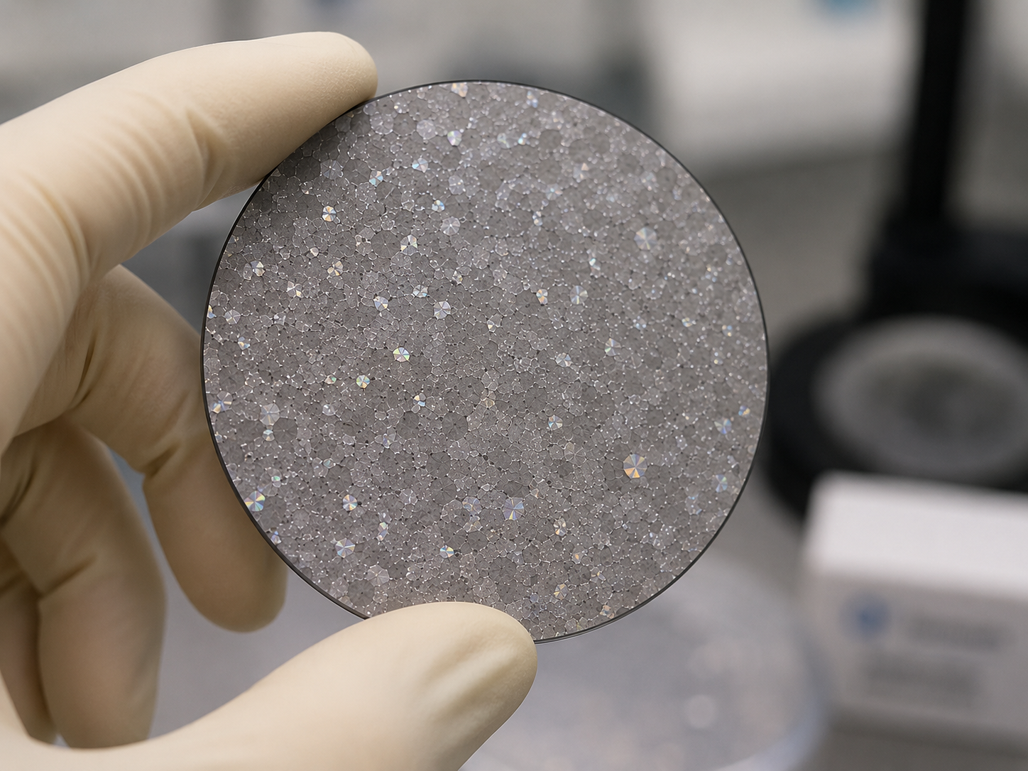
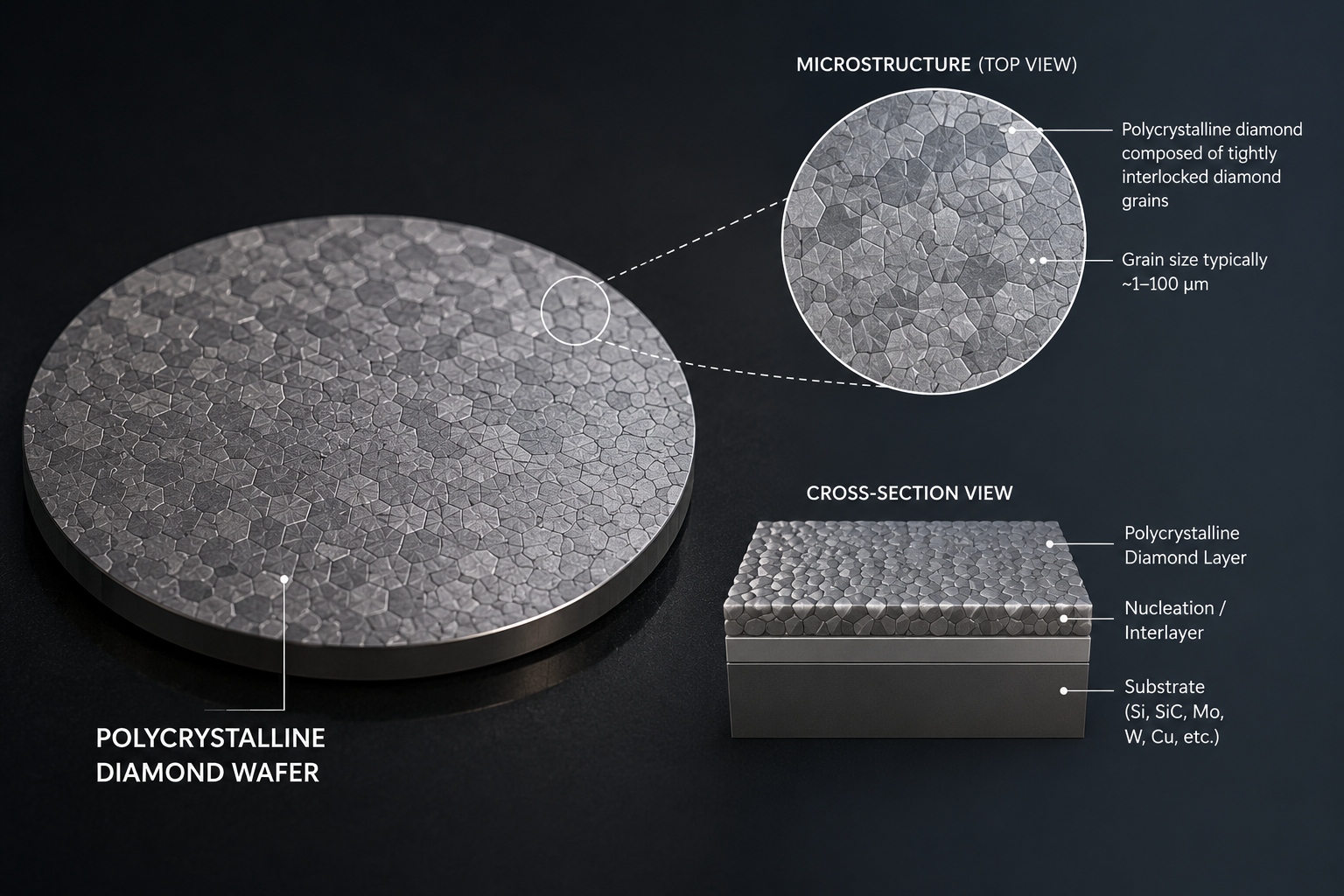
polycrystalline diamond wafer

Polycrystalline Diamond Wafer Solutions for Semiconductor & Thermal Management Applications
Q² Diamonds supplies high-performance polycrystalline diamond wafers engineered for semiconductor, RF, photonics, quantum, and high heat flux applications.
Our synthetic CVD diamond wafers deliver ultra-high thermal conductivity, low thermal expansion, and scalable manufacturing for advanced electronic packaging and thermal management systems.
Datasheets, technical specifications, sample availability, and application discussions for OEMs, semiconductor companies, research labs, and advanced packaging teams.
- ✔ Polycrystalline CVD diamond wafers up to 2200 W/m·K
- ✔ Custom wafer sizes, polishing, metallisation & substrate engineering
- ✔ For semiconductor, RF, photonics & thermal applications
- ✔ Scalable synthetic diamond manufacturing with competitive cost structure
- ✔ UK & Europe technical-commercial support via Q² Diamonds
What is a Polycrystalline Diamond Wafer?
A polycrystalline diamond wafer is a synthetic diamond substrate manufactured using chemical vapour deposition (CVD) technology. These diamond wafers are engineered for applications requiring exceptional thermal conductivity, thermal stability, and heat spreading performance.
Compared to conventional materials such as copper, aluminium, AlSiC, and ceramic substrates, polycrystalline diamond wafers offer significantly higher thermal conductivity — reaching up to 2200 W/m·K — while maintaining low thermal expansion and excellent material stability.
Q² Diamonds manufactures CVD polycrystalline diamond wafers for semiconductor packaging, GaN and SiC devices, RF electronics, laser systems, photonics, aerospace, quantum technologies, and advanced thermal management applications.
Custom wafer dimensions, metallisation, polishing, and engineered composite integration are available for OEMs, research institutions, and advanced electronics manufacturers across the UK and Europe.
Why Use Polycrystalline Diamond Wafers?
As semiconductor power densities continue to increase, conventional substrate and thermal management materials are reaching performance limitations. Polycrystalline diamond wafers provide superior thermal conductivity, reduced thermal resistance, and improved reliability for next-generation electronic systems.
Superior Thermal Conductivity
Improved Reliability & Reduced Thermal Stress
Low Coefficient of Thermal Expansion
Advanced Semiconductor Packaging Compatibility
Scalable Synthetic Diamond Wafer Manufacturing
Applications of Polycrystalline Diamond Wafers
Polycrystalline diamond wafers are used in high-performance semiconductor and photonic systems where thermal limits directly impact device reliability, efficiency, and power density.
GaN & SiC Power Electronics
Diamond wafers improve thermal management in high-power GaN and SiC semiconductor devices used in EVs, renewable energy systems, RF amplifiers, and industrial converters.
RF & Microwave Packaging
Polycrystalline diamond substrates enable efficient heat spreading in radar systems, satellite communications, telecom infrastructure, and high-frequency RF electronics.
Photonics & Laser Systems
Synthetic diamond wafers provide thermal stability for laser diodes, optical systems, and photonics applications requiring precise temperature control.
AI Hardware & Data Centres
Diamond wafer substrates support high heat flux management for GPUs, AI accelerators, and next-generation computing infrastructure.
Quantum & Research Applications
Used in advanced research environments where thermal conductivity, stability, and material performance are critical.
Supporting OEMs, research labs, and system designers across the UK and Europe.
Q² Polycrystalline Diamond Wafer Solutions
Q² Diamonds manufactures synthetic polycrystalline diamond wafers and engineered diamond thermal management materials for semiconductor, photonics, RF, aerospace, and advanced packaging applications.
CVD Polycrystalline Diamond Wafers
High thermal conductivity synthetic diamond wafers engineered for semiconductor cooling, heat spreading, and advanced electronic packaging.
Metallised Diamond Substrates
Custom metallisation and bonding layers designed for integration into RF, photonics, and semiconductor assemblies.
Copper–Diamond Composite Materials
Engineered Cu–Diamond composites combining thermal performance with scalable manufacturing and integration flexibility.
Custom Diamond Wafer Manufacturing
Tailored wafer dimensions, polishing, thicknesses, and substrate engineering for OEM and research requirements.